


- Stock: 1
- Marque: IteadStudio
- Modèle: DZD000164
- Poids: 40.00g
- Dimensions: 38.00mm x 38.00mm x 30.00mm
Description :
Module de caméra VGA FIFO OV7670 Carte de capteur d'image Pixel 30W Pilote de microcontrôleur STM32 pour kit de bricolage Arduino
La caméra FIFO a plus qu'un cache 3M, qui peut stocker temporairement les données collectées dans ce cache. Lors de l'utilisation, il peut lire les données d'image dans le cache, de sorte qu'il peut réduire la vitesse MCU lorsque le microcontrôleur capture des données d'image. La demande. (La routine stocke les données d'image en mode RGB565)
1. Aperçu du produit
OV7670 avec le module de FIFO est un genre de module avec l'espace mémoire tampon pour MCU lent pour réaliser le contrôle d'acquisition d'image. Ce module ajoute une puce mémoire FIFO (first-in, first-out), qui contient également un capteur d'image CMOS de 30 pixels, une monture d'objectif à distance focale de 3.6mm, et une monture d'objectif. Diverses alimentations à bord sont nécessaires pour la puce CMOS. Le fichier de données de la puce), la carte mène également à la broche de contrôle et à la broche de données, ce qui est pratique pour le fonctionnement et l'utilisation.
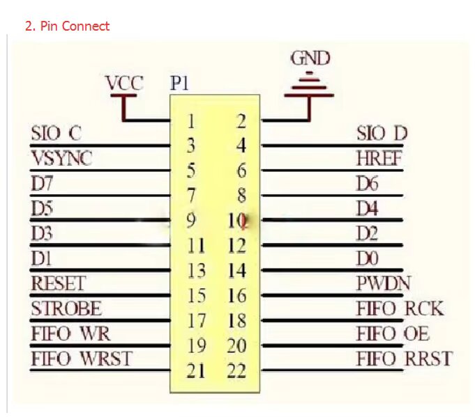
3V3: Tension d'alimentation d'entrée (3.3 V est recommandé mais non recommandé)
GDN: Point de mise à la terre
SIO_C: horloge de contrôle de l'interface SCCB (Remarque: certains microcontrôleurs de bas niveau nécessitent un contrôle pull-up, similaire à l'interface I2C)
SIO_D: côté entrée (sortie) des données série de l'interface SCCB (Remarque: certains microcontrôleurs de bas niveau nécessitent un contrôle pull-up, similaire à l'interface I2C)
VSYNC: Signal de synchronisation de trame (signal de sortie)
HREF: Signal de synchronisation de ligne (signal de sortie, généralement non applicable, circonstances spéciales)
D0-D7: Port de données (signal de sortie)
RESTE: réinitialiser le port (utilisation normale tirer haut)
PWDN: mode de sélection de la consommation d'énergie (utilisation normale tirer bas)
STROBE: port de contrôle du flash de l'appareil photo (une utilisation normale peut ne pas être nécessaire)
FIFO_RCK: Contrôleur d'horloge de lecture de mémoire FIFO
FIFO_WR_CTR: Contrôle d'écriture FIFO (1 pour activer l'écriture CMOS sur FIFO, 0 est désactivé)
FIFO_OE: Contrôle d'arrêt FIFO
FIFO_WRST: réinitialisation du pointeur d'écriture FIFO
FIFO_RRST: réinitialisation du pointeur de lecture FIFO
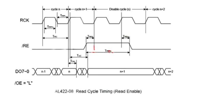
3. Instructions de contrôle
Parce que FIFO est utilisé comme mémoire tampon de données, la collecte de données est simple et pratique. Les utilisateurs doivent seulement se soucier de la façon de lire, et n'ont pas besoin de se soucier de la façon dont des données spécifiques sont collectées. Cela peut réduire ou même éliminer les relations de contrôle et de synchronisation CMOS. Il est capable de réaliser l'acquisition d'images.
La séquence de contrôle est la suivante:


")
")


